VC2301HX-2.3A
Weforsemi
P-Channel 20V(D-S) MOSFET
| Material: | |
|---|---|
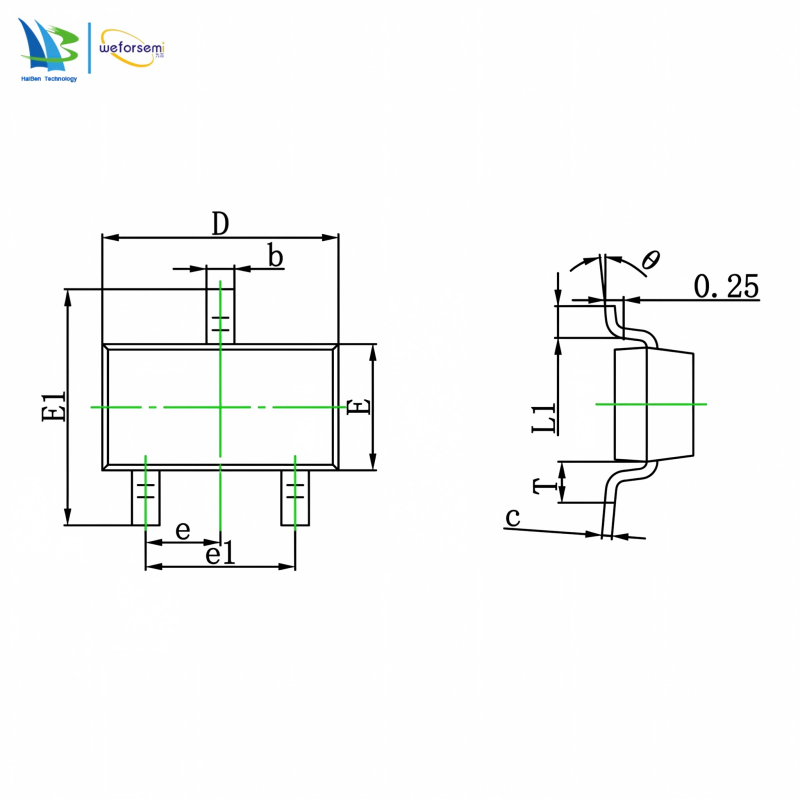
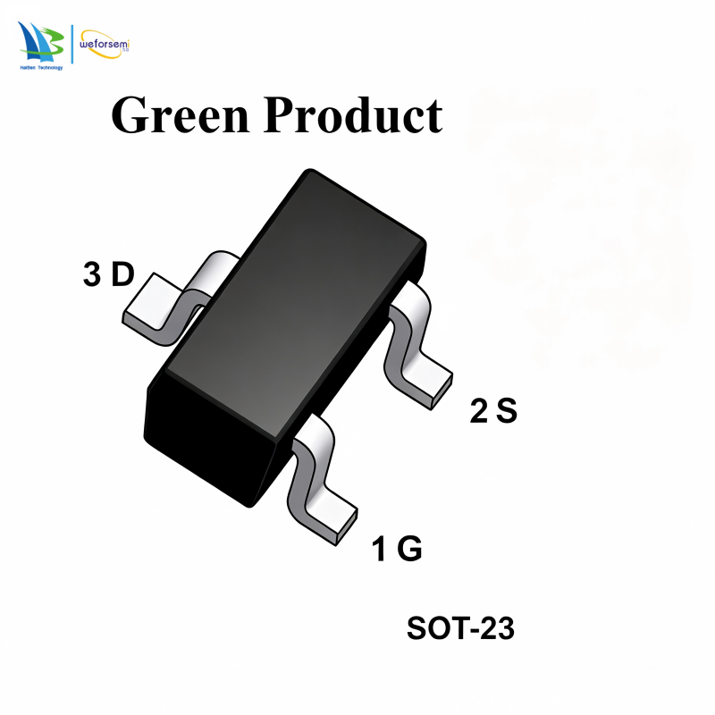
| Package:: | |
| Type: | |
| Specification: | |
| Feature: | |
| Application1: | |
| Application2: | |
| Availability: | |
| Quantity: | |
Electronic Component Factory SOT-23 P-Channel MOSFET VC2301HX-2.3A Semiconductor of MOSFETS OEM Electronics Manufacturer
Configuration
VDSS= -20 V ID= -2.3 A
RDS(on) < 150mΩ@VGS =-4.5V
RDS(on) < 175mΩ@VGS =-2.5V
Feature
TrenchFET Power MOSFET
Application
Load Switch for Portable Devices
DC/DC Converter
Maximum ratings (Ta=25ºC unless otherwise noted)
| Parameter | Symbol | Value | Unit |
| Drain-Source Voltage | VDS | -20 | V |
| Gate-Source Voltage | VGS | ±8 | |
| Continuous Drain Current | ID | -2.3 | A |
| Pulsed Drain Current | IDM | -10 | |
| Continuous Source-Drain Diode Current | IS | -0.72 | |
| Maximum Power Dissipation | PD | 0.4 | W |
| Thermal Resistance from Junction to Ambient(t ≤5s) | R θJA | 312.5 | ºC/W |
| Junction Temperature | TJ | -55 ~+150 | ºC |
| Storage Temperature | Tstg | -55 ~+150 |
MOSFET ELECTRICAL CHARACTERISTICS
Ta =25 ºC unless otherwise specified
| Parameter | Symbol | Test Condition | Min | Typ | Max | Units | |
| Static | |||||||
| Drain-source breakdown voltage | V(BR)DSS | VGS = 0V, ID =-250µA | -20 | V | |||
| Gate-source threshold voltage | VGS(th) | VDS =VGS, ID =-250µA | -0.4 | -0.7 | -1 | ||
| Gate-source leakage | IGSS | VDS =0V, VGS =±8V | ± 100 | nA | |||
| Zero gate voltage drain current | IDSS | VDS =-20V, VGS =0V | -1 | µA | |||
| Drain-source on-state resistance a | RDS(on) | VGS =-4.5V, ID =-2.3A | 125 | 150 | m Ω | ||
| VGS =-2.5V, ID =-2.0A | 142 | 175 | |||||
| Forward transconductance a | gfs | VDS =-5V, ID =-2.3A | 6.5 | S | |||
| Dynamicb | |||||||
| Input capacitance | Ciss | VDS =-10V,VGS =0V,f =1MHz | 405 | pF | |||
| Output capacitance | Coss | 75 | |||||
| Reverse transfer capacitance | Crss | 55 | |||||
| Total gate charge | Qg | VDS =-10V,VGS =-4.5V,ID =-2.3A | 5.5 | nC | |||
VDS =-10V,VGS =-2.5V,ID =-2.3A | 3.3 | ||||||
| Gate-source charge | Qgs | 0.7 | |||||
| Gate-drain charge | Qgd | 1.3 | |||||
| Gate resistance | Rg | f =1MHz | 6.0 | Ω | |||
| Turn-on delay time | td(on) | VDD=-10V, RL=10Ω , ID =-1A, VGEN=-4.5V,Rg=1Ω | 11 | 2 | ns | ||
| Rise time | tr | 35 | 6 | ||||
| Turn-off delay time | td(off) | 30 | 5 | ||||
| Fall time | tf | 10 | 2 | ||||
| Drain-source body diode characteristics | |||||||
| Continuous source-drain diode current | IS | TC=25ºC | -1.3 | A | |||
| Pulse diode forward current a | ISM | -10 | |||||
| Body diode voltage | VSD | IS=-0.7A | -0.8 | -1.2 | V | ||