3.1W Mono Audio IC Single-Channel Class AB/D Power Amplifier Chip Integrated Circuit Manufacturer
Features
1. Class AB/Class D switching function
2. Two anti-clipping options, anti-clipping compression range -10dB
3. Class D output power:
-3.1W (VDD=5.0V, RL =4Ω, THD+N=10%) -1.8W (VDD=5.0V, RL =8Ω, THD+N=10%)
4. Class AB output power:
-3.0W (VDD=5.0V, RL =4Ω, THD+N=10%) -1.7W (VDD=5.0V, RL =8Ω, THD+N=10%)
5. Operating voltage: 2.5V to 5.5V
6. Low distortion and low noise
7.POP-click suppression function on/off
8. Shutdown current (<1uA)
9. OCP, OTP, UVLO protection functions
Applications
1.Watches, wristbands
2.Smart glasses
3.Bone conduction headphones
Product Highlights
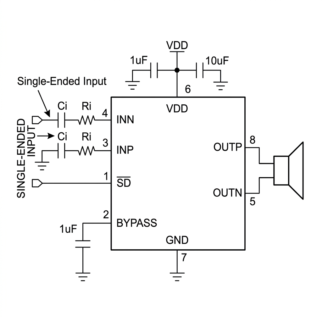
The VC2033 is an FM interference-free, anti-clipping, switchable AB/D class, high-efficiency, filterless 3.1W mono audio power amplifier. Its ultra-small package makes it ideal for wearable devices.
The VC2033's differential input architecture and extremely high PSRR effectively improve its RF noise suppression capabilities. The filterless PWM modulation structure and built-in gain reduce external components, PCB area, and system cost, simplifying design. Up to 90% efficiency, fast startup time, and a small package size make the VC2033 an optimal choice for portable audio products.
The VC2033 features extremely low shutdown current, significantly extending system standby time. OCP, OTP, and UVLO protection enhance system reliability. On/off pop-click suppression improves the listening experience and simplifies system setup.
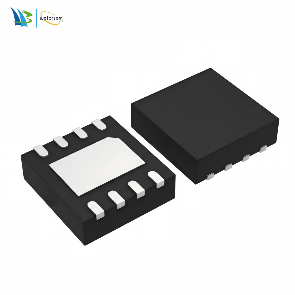
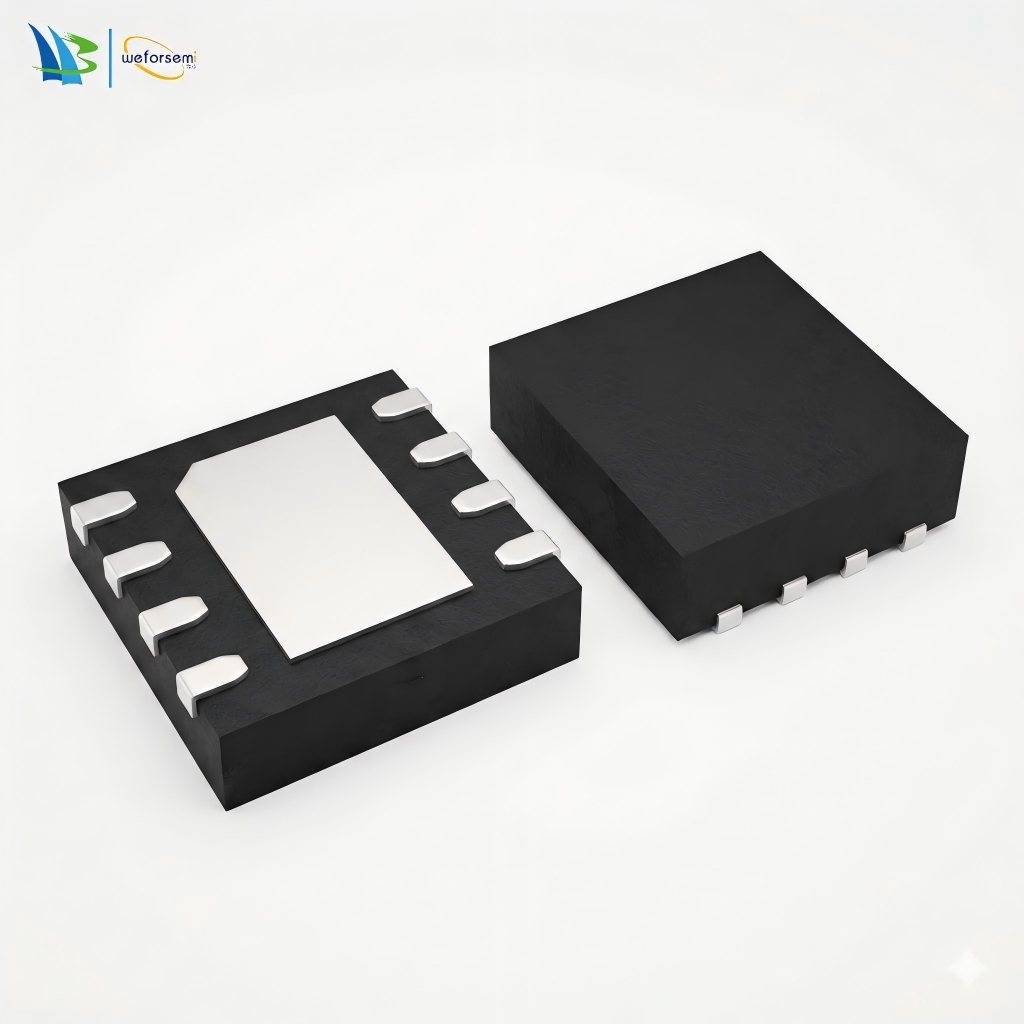
The VC2033 is available in a DFN2X2_8L package with a heatsink.
CLASS D Mode Electrical Characteristics
(VDD =5V, Gain=23dB, RL =4Ω T =25°C, unless otherwise noted.)
| Symbol | Parameter | Test Conditions | MIN | TYP | MAX | UNIT |
| VIN | Supply Voltage |
|
| 2.5 | - | 5.5 | V |
PO |
Class-D Mode Output Power | THD+N=10%,f=1KHZ,RL=4Ω | VDD=5.0V |
| 3.1 |
| W |
| VDD=3.6V |
| 1.7 |
|
| THD+N=1%,f=1KHZ,RL=4Ω | VDD=5.0V |
| 2.6 |
| W |
| VDD=3.6V |
| 1.45 |
|
| THD+N=10%,f=1KHZ,RL=8Ω | VDD=5.0V |
| 1.8 |
| W |
| VDD=3.6V |
| 1.05 |
|
| THD+N=1%,f=1KHZ,RL=8Ω | VDD=5.0V |
| 1.5 |
| W |
| VDD=3.6V |
| 0.87 |
|
THD+N |
THD+N | VDD=5.0V, PO=0.5W, RL=4Ω | f=1KHz |
| 0.02 |
| % |
| VDD=3.6V, PO=0.5W, RL=4Ω |
| 0.05 |
|
| VDD=5.0V, PO=0.5W, RL=8Ω | f=1KHz |
| 0.02 |
| % |
| VDD=3.6V, PO=0.5W, RL=8Ω |
| 0.03 |
|
| GV | Class-D Mode Gain |
| Ri = 22K |
| 23 |
| dB |
| PSRR | PSRR | VDD=4.2V ±200mVp-p | f=1KHz |
| 60 |
| dB |
| SNR | SNR | VDD=5.0V, Vo rms=1V,
GV=22dB | f=1KHz |
| -82 |
| dB |
Vn |
Residual Noise | VDD=5.0V,Input floating with CIN=0.1μF | A-weighting |
| 73 |
|
μV |
No
A-weighting |
| 100 |
|
| Dyn | Dynamic Range | VDD=5.0V,THD=1% | f=1KHz |
| -89 |
| dB |
η | Efficiency | RL=4Ω, Po=1W | f=1KHz |
| 85 |
| % |
| RL=4Ω, Po=2W |
| 90 |
|
| IQ | Quiescent Current | VDD=5.0V | No Load |
| 6 |
| mA |
| VDD=3.0V |
| 3 |
|
| ISD | Shutdown Current | VDD=2.5V to 5V | VSD=0.3V |
|
| 1 | μA |
| Vos | Offset Voltage | VIN=0V, VDD=5V |
|
| 10 | 40 | mV |
| Fosc | Operating Frequency |
|
|
| 600 |
| khz |
| Tst | Startup Time | Bypass capacitor =1uF |
|
| 180 |
| mS |
| OTP | - | No Load,Junction Temperature | VDD=5.0V |
| 165 |
| °C |
| OTH | - |
| 40 |
|