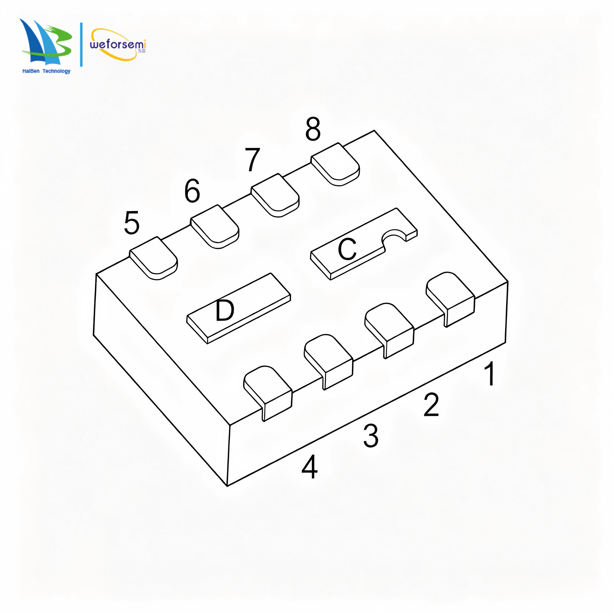
Production manufacturer DFNWB3×2-08L-B Power Composite Integrated VC2301A MOSFET-Schottky Diode Semiconductor
FEATURES
• Independent Pinout to Each Device to Ease Circuit Design
• Ultra low VF
• Including a VC2301A MOSFET and a VC0520B Schottky
(independently) in a package
APPLICATIONS
• Li−Ion Battery Charging
• High Side DC−DC Conversion Circuits
• High Side Drive for Small Brushless DC Motors
Power Management MOSFETS-Schottky
| V(BR)DSS/VR | RDS(on) MAX | ID/IO |
-20V | 110mΩ@-4.5V |
-2.7A |
| 160mΩ@-2.5V |
| 240mΩ@-1.8V |
| 20V | / | 1 A |
MAXIMUM RATINGS (Ta=25ºC unless otherwise noted)
| Symbol | Parameter | Value | Unit |
| P-MOSFET |
| VDS | Drain-Source Voltage | -20 | V |
| VGS | Gate-Source Voltage | ±8 | V |
| ID | Continuous Drain Current | -2.7 | A |
| IDM* | Pulse Drain Current | -10 | A |
| Schottky Barrier Diode |
| VRRM | Peak Repetitive Reverse Voltage | 20 | V |
| VR | DC Blocking Voltage | 20 | V |
| IO | Average Rectified Forward Current | 1 | A |
| Power Dissipation, Temperature and Thermal Resistance |
| PD | Power Dissipation | 1.1 | W |
| RθJA | Thermal Resistance from Junction to Ambient | 114 | ºC/W |
| Tj | Junction Temperature | 150 | ºC |
| Tstg | Storage Temperature | -55~+150 | ºC |
| TL | Lead Temperature for Soldering Purposes(1/8'' from case for 10 s) | 260 | ºC |
ELECTRICAL CHARACTERISTICS
Ta =25 ºC unless otherwise specified
| Parameter | Symbol | Test conditions | Min | Typ | Max | Unit |
| P-MOSFET |
| STATIC PARAMETERS |
| Drain-source breakdown voltage | V (BR)DSS | VGS =0V, ID=-250µA | -20 |
|
| V |
| Zero gate voltage drain current | IDSS | VDS =-16V,VGS = 0V |
|
| -1 | µA |
| Gate-body leakage current | IGSS | VGS =±8V, VDS = 0V |
|
| ±100 | nA |
| Gate threshold voltage | VGS(th) | VDS =VGS, ID =-250µA | -0.45 |
|
| V |
Drain-source on-resistance(note1) |
RDS(on) | VGS =-4.5V, ID =-2.7A |
|
| 110 | mΩ |
|
| VGS =-2.5V, ID =-2.2A |
|
| 160 | mΩ |
|
| VGS =-1.8V, ID =-1A |
|
| 240 | mΩ |
| Forward transconductance(note1) | gFS | VDS=-10V,ID=-2.7A |
| 7 |
| S |
| Diode forward voltage(note1) | VSD | IS=-0.9A, VGS = 0V |
|
| -1.2 | V |
| DYNAMIC PARAMETERS (note 2) |
| Input capacitance | Ciss |
VDS =-10V,VGS =0V,f =1MHz |
|
| 300 | pF |
| Output capacitance | Coss |
|
|
| 150 | pF |
| Reverse transfer capacitance | Crss |
|
|
| 50 | pF |
| SWITCHING PARAMETERS (note 2) |
| Turn-on delay time | td(on) |
VGS=-4.5V,VDD=-10V,
RL=10Ω,RG=6Ω , ID=-1A |
|
| 25 | ns |
| Turn-on rise time | tr |
|
|
| 45 | ns |
| Turn-off delay time | td(off) |
|
|
| 45 | ns |
| Turn-off fall time | tf |
|
|
| 40 | ns |
| Total Gate Charge | Qg | VDS =-10V,VGS =-4.5V, ID =-2.7A |
|
| 6.5 | nC |
| Gate-Source Charge | Qgs |
|
| 1.4 |
| nC |
| Gate-Drain Charge | Qgd |
|
| 0.65 |
| nC |
| SCHOTTKY BARRIER DIODE |
| Forward voltage | VF | IF=0.5A |
|
| 0.48 | V |
| Reverse current | IR | VR=20V |
|
| 100 | µA |
| Junction capacitance | Cj | VR=10V,f=1MHz |
| 41 |
| pF |