VCTB3V32515LC
Weforsemi
VCTB3V32515LC
| Material: | |
|---|---|
| Structure: | |
| Package Structure: | |
| Working Frequency: | |
| Operating Voltage: | |
| Peak Pulse Power: | |
| Peak Pulse Current: | |
| Availability: | |
| Quantity: | |
Manufacturer Advanced Design Bidirectional Dfn0603-2 Tvs Diode Vctb3V32515LC Integrated Circuit
Description
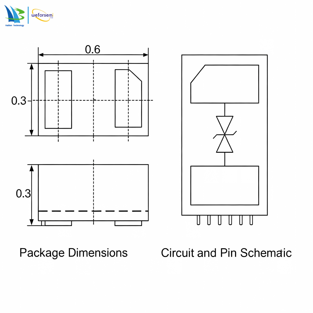
The VCTB3V32515LC is a bi-directional TVS diode, utilizing leading monolithic silicon technology to provide fast response time and low ESD clamping voltage, making this device an ideal solution for protecting voltage sensitive data and power lines. The VCTB3V32515LC complies with the IEC 61000-4-2 (ESD) with ±30 kV air and ±30 kV contact discharge. It is assembled into an ultra-small 0.6x0.3x0.3mm lead-free DFN package. The ultra-small size and high ESD surge protection make VCTB3V32515LC an ideal choice to replace 0201-size multilayer varistors (MLVs) and protect cell phones, digital cameras, audio players and many other portable applications.
Features
Ultra small package: 0.6x0.3x0.3mm
Very low capacitance
Protects one data or power line
Ultra low leakage: nA level
Operating voltage: 3.3V
Low clamping voltage
2-pin leadless package
Complies with the following standards:
- IEC 61000-4-2 (ESD) immunity test Air discharge: ±30kV
Contact discharge: ±30kV
- IEC61000-4-5 (Lightning) 8A (8/20μs)
RoHS Compliant
Applications
Cellular Handsets and Accessories
Personal Digital Assistants
Notebooks and Handhelds
Portable Instrumentation
Digital Cameras
Peripherals
Audio Players
Keypads, Side Keys, USB 2.0, LCD Displays
Absolute Maximum Ratings (TA=25°C unless otherwise specified)
Peak Pulse Power (8/20μs):Ppk = 80 W
Peak Pulse Current (8/20μs):Ipp = 8 A
ESD per IEC 61000 4-2 (Air) / (Contact):VESD = ±30 kV
Operating Temperature Range (TJ):-55 to +125 ºC
Storage Temperature Range (Tstg):-55 to +150 ºC


content is empty!